Ionisation induced in semiconductor materials or associated insulators, such as silicon dioxide layers, can lead to charge trapping or the formation of interface states at the semiconductor‐insulator boundary, affecting component behaviour or material properties. In MOS devices, the trapped charge can lead to a shift in the gate threshold voltage, and for semiconductors in general, interface states can significantly increase device leakage currents. Materials such as polymers and glasses are also susceptible to total ionising dose (TID) effects and can suffer degradation in mechanical, electrical and optical properties.
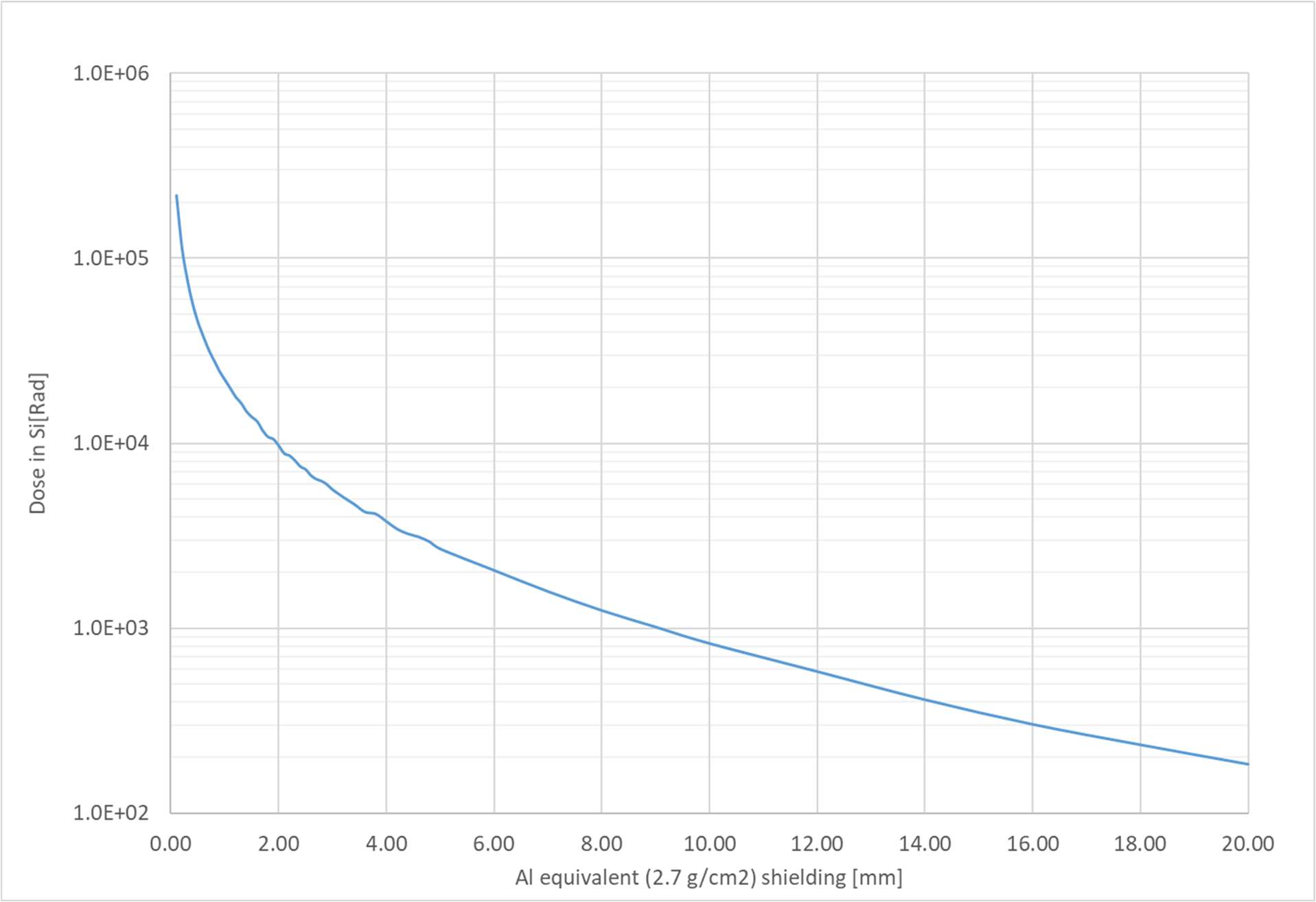
The ionizing dose environment is represented by the dose-depth curve. This may provide dose as a function of shield thickness in planar geometry or as a function of spherical shielding about a point. The planar model is appropriate for surface materials or for locations near to a planar surface. In general, electronic components are not in such locations and a spherical model is recommended for general specification.